Descriptive Text of Value Chain Step
In this value chain, we focus on utility-scale solar power generated using photovoltaic (PV) technology. PV cells convert solar radiation to electric energy when photons (particles of light) knock electrons free from atoms, generating a flow of electricity; this process is known as the photovoltaic effect. The power generated in a utility PV system is typically distributed by an electric utility or routed to the wholesaler power market.
PV technologies have evolved over time and can be classified into three generations based on the basic material used and their level of commercial maturity.
- “First-generation PV” refers to crystalline silicon PV technology, of which the two most common types are monocrystalline silicon PV cells (mono c-Si) and polycrystalline silicon PV cells (poly c-Si). These technologies are widely commercially available.
- “Second-generation PV” refers to early adopted thin-film PV technologies; in these PV cells, layers of semiconductor materials are deposited directly on a substrate. Types of semiconductor materials include amorphous and micromorph silicon (a-Si/mc-Si), copper indium diselenide (CIS), copper indium gallium diselenide (CIGS), or cadmium telluride (CdTe). Among these different materials, a-Si solar cells and CdTe cells are the most developed and widely used in thin-film PV.
- “Third-generation PV” refers to solar technologies still undergoing research and development and not yet widely deployed; this category includes concentrating PV (CPV), dye-sensitized solar cells (DSSC), and organic PV cells.
Table DI.1 Generations of PV Technologies
Source: Recreated from Table 3 in Lacerda et al., 2016 Diversity in solar photovoltaic energy: Implications for innovation and policy
| PV solar generation | Technology alternatives | Year of first best research-cell efficiency reports |
| 1st | Mono-crystalline | 1954 |
| Multi-crystalline | 1984 | |
| 2nd | Amorphous silicon (a-Si) | 1976 |
| Multi-junction thin silicon film (a-Si/µc-Si) | 1976 | |
| Cadmium telluride (CdTe) | 1976 | |
| Copper, indium, gallium, (di) selenide/(di)sulfide (CIGS) | 1976 | |
| 3rd | Organic PV (OPC) | 2001 |
| Dye-sensitized solar cell (DSCC) | 1991 |
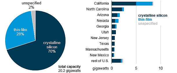
Historically, U.S. utility-scale PV has been dominated by crystalline silicon PV technology, in terms of installed capacity. In 2016, almost 70% of total came from crystalline silicon PV modules; thin-film PV modules represented about 28% of new solar capacity (see Figure D.1). Therefore, we focus on crystalline silicon PV modules and thin-film PV modules in this “module manufacturing” value chain step.

Figure DI.1 U.S. Solar PV Capacity by PV Technology in 2016
Source: U.S. Energy Information Administration https://www.eia.gov/todayinenergy/detail.php?id=34112
(original data from U.S. EIA, Annual Electric Generator Report)
Crystalline silicon PV module manufacturing involves multiple steps. First, polysilicon processing takes place. Once polysilicon is produced, it is formed into ingots, which are sliced into thin wafers. The wafers are then assembled into solar cells. The finished solar cells are laminated within encapsulants and sandwiched between a glass layer and a protective backsheet. The encapsulated solar cells are then placed into an aluminum frame; a junction box connecting the cells to form an electric circuit is added to complete the PV module.
Depending on the way crystalline silicon is processed to make wafers, c-Si PV cells can be divided into two sub-categories: polycrystalline PV cells and monocrystalline PV cells. To manufacture polycrystalline PV cells, the most common form of PV technology, the ingots are made by melting multiple silicon crystals together and casting in a cube mold; the ingot is then cooled and cut into square-shaped wafers. This melting process distorts the silicon’s crystal structure, giving polycrystalline PV cells a distinctive blue color. A string ribbon solar cell is a type of poly c-Si that utilizes ribbon processing, where thin ribbons or sheets of polycrystalline silicon are drawn from a polysilicon melt, to reduce silicon waste. To make monocrystalline PV cells, silicon with a single, continuous crystal structure is pulled into a cylindrical-shaped ingot via the Czochralski process. To maximize space on solar modules, four sides are cut out of the cylindrical ingots before slicing into wafers, which gives the monocrystalline PV cells its characteristic shape (see Figure DI.2).
As compared to crystalline silicon PV modules, the manufacturing process of thin-film PV modules is much simpler and requires only a single step. The process starts from depositing thin layers of semiconductor materials, like amorphous silicon (a-Si), copper indium selenide (CIS), copper indium gallium selenide (CIGS), or cadmium telluride (CdTe), on a substrate, which can either be glass, polymer or metal. The film will then be structured into cells. The film layer ranges between a few nanometers to tens of micrometers in thickness, which is about 100 times thinner than crystalline silicon cells. This feature allows thin-film cells to be flexible. Thin-film PV modules are usually less costly to produce than crystalline silicon systems due to their lower production and material costs (up to 99% less material than crystalline solar cells for the same amount of sunlight absorbed).
![]()
Figure DI.2 Crystalline Silicon PV Modules and Thin-Film PV Modules
Source: Clean Energy Review https://www.cleanenergyreviews.info/blog/pv-panel-technology
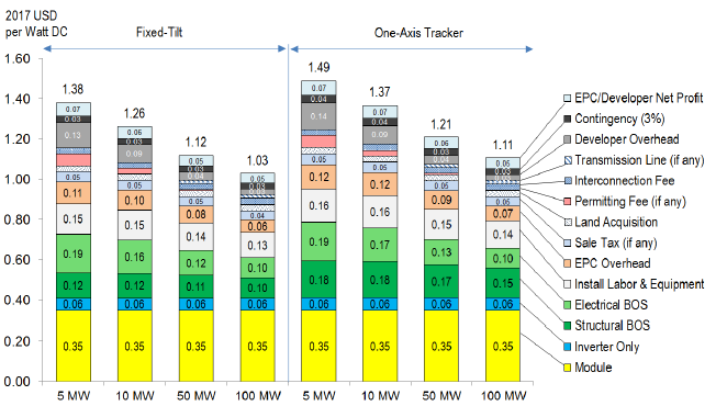
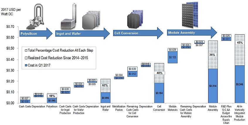
In a recent report, NREL estimated that c-Si PV modules cost approximately $0.35 per WattDC, accounting for 31.5% of the total system cost for a 100 MW capacity utility-scale PV project with one-axis tracker system (total cost: $1.11 per WattDC). In their bottom-up manufacturing cost model, the polysilicon represents 13.3% of the module cost; the wafer represent 14.7% of the module cost; the cell represent 25.4% of the module cost; the rest of the cost occurs for module assembly. In thin-film modules, material costs are lower as compared to crystalline silicon modules. However, other components such as mounting systems may be more expensive per kWp, as more space is required.
Solar glass is also an important component in solar modules; it is used to protect and enhance performance of modules and often serves as a substrate for thin-film modules. Ultra-clear glass is required to maintain high efficiency performance in solar modules. Lower grade glass can cloud over time and results in degraded solar efficiency. Flat glass is the most common glass type used in solar modules; however, given the current solar glass production level, it is difficult for glass manufacturers to be dedicated strictly to solar glass. Typically, solar glass production accounts for a very small portion of glass manufacturers’ total business.
The PV module manufacturing step in the value chain is covered by “Semiconductor and Related Device Manufacturing” (NAICS 334413) . As reported in 2012 Economic Census, there are 862 establishments and 102,570 employees covered under this industry, with a value of shipments of 48,613 million dollars. However, even at their most disaggregated level (six-digit codes), NAICS codes cover a range of components, products or services that are not specific to PV module manufacturing.
Figure DI.3 shows the cost breakdown of various types of utility-scale solar projects based on NREL’s estimates, and Figure DI.4 illustrates a bottom-up manufacturing cost model for crystalline silicon PV modules.

Figure DI.3 Utility-Scale PV System Cost Breakdown
Source: Figure 28 from NREL Solar PV System Cost Benchmark Q1 2017

Figure DI.4 Bottom-up Manufacturing Cost Model Results for Crystalline Silicon PV Module Supply Chain
Source: Figure 11 from NREL Solar PV System Cost Benchmark Q1 2017